
One Trapped Ion Now Maps the Fields That Break Quantum Chips


Researchers at ETH Zurich have turned a single trapped ion into a tool that measures electromagnetic fields just above a chip’s surface and builds a three-dimensional map of them. The stray fields it detects are the same ones that degrade the quantum states inside ion-trap quantum computers and sensors. The work, led by physicist Jonathan Home, was published in the journal Science Advances.
How one beryllium ion becomes a field scanner
According to the ETH Zurich’s report, modern ion traps have shrunk from bulky lab instruments into miniaturized chips that hold ions a hair’s breadth above the surface. That closeness helps in most ways and hurts in one. Noisy electromagnetic fields coming off the chip itself disturb the fragile quantum states the whole system depends on, and for a long time nobody could say exactly where that noise came from.
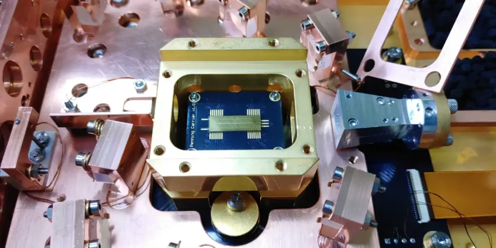
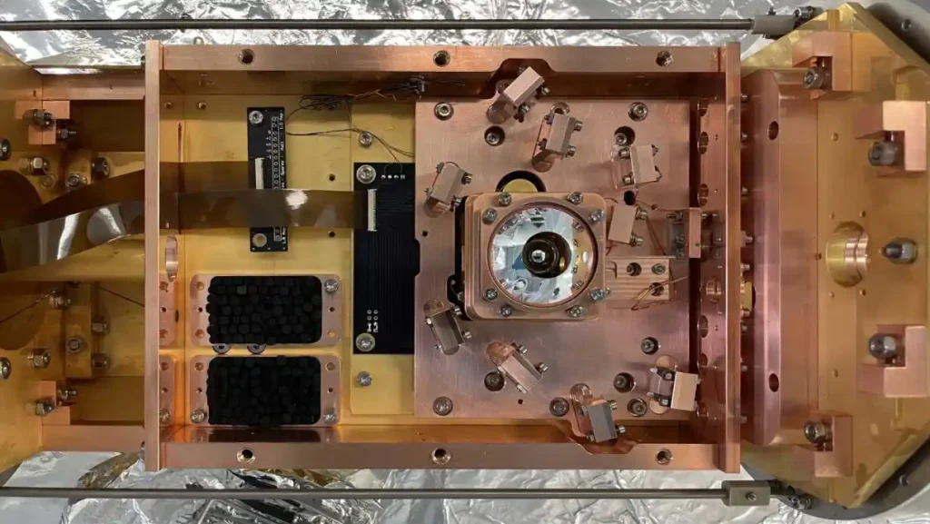
Home’s group attacks the problem with a Penning trap, which holds the ion using static electric and magnetic fields rather than the oscillating radio-frequency fields most traps rely on. The team built the underlying chip trap two years ago, and it does something conventional traps cannot. It moves a single ion anywhere in three dimensions above the chip. Doctoral student Shreyans Jain says the design carries two benefits. The ion can be placed freely in 3D, and because there are no oscillating fields inside the trap, tiny oscillating fields on the chip become far easier to spot.
Cooling the ion, then steering it into position
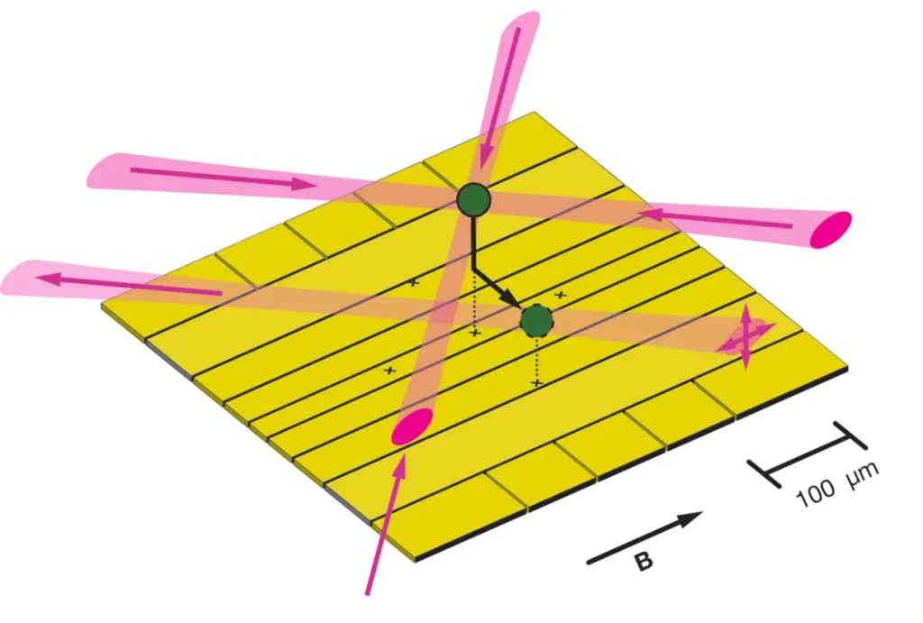
The measurement itself reads like slow, careful choreography. First the researchers cool a beryllium ion with laser beams until it reaches its lowest quantum mechanical oscillation state and effectively sits still. Then they adjust the voltages on the trap electrodes to steer the ion to a chosen spot. “We can vary the height above the chip from 50 micrometres up to 450 micrometres and scan an area of 200 by 200 micrometres,” says doctoral student Tobias Sägesser. Once the ion arrives, they wait. Oscillating fields on the chip nudge it into swinging back and forth more and more strongly, which shifts its quantum oscillation state, and laser pulses read out that shift after a set waiting time. From the change, the team calculates the strength of the disturbing field.
The sensitivity is the headline. Sägesser says they set a record for the most sensitive measurement of an oscillating electric field in a chip trap, detecting a field of just 10 nanovolts per meter within a one-second measurement. To picture how faint that is, the field from a mobile phone several kilometres away is still ten thousand times stronger. The same setup handles other fields too. Static electric fields show up as a visible deflection of the ion under a microscope, and magnetic fields register as changes in the ion’s energy levels.
Why quantum chip makers need this
The point of a 3D field map is to fix chips before they ever hold a qubit in earnest. “For more than thirty years, researchers have tried to find out where the electric field noise close to a chip comes from,” Home says. His method measures those fields precisely and with spatial resolution in all three dimensions, then compares the readings against model calculations, which lets the team separate one possible source of interference from another. The Penning trap can also be cut off entirely from outside voltage sources, so environmental influences can be ruled out instead of assumed. Home notes that until now people had to guess at those influences without knowing whether their assumptions held.
He sees the technique becoming a standard way to characterize materials. Ions can scan regions of a chip made from different surface materials to find which one produces the smallest fields, and that information can feed back into the chip manufacturing process. Better materials and cleaner processes mean quieter chips, and quieter chips are what ion-trap quantum computers and sensors need to work reliably.